GD32F103 (GigaDevice) — chip + Blue-Pill-compatible boards
⚡ The essentials in 60 seconds
- mcu_cpu — Arm Cortex-M3, 32-bit, up to 108 MHz with zero-wait-state flash accesses (vs 72 MHz on the ST STM32F103 — see Features). Zero-wait applies to the first 256 KB of flash only (GD32F10x User Manual EN V2.3 §2.1, mirror).
- gpu — none (MCU).
- ram — 6/10/20 KB SRAM on 16–128 KB parts (T/C/R/V 4/6/8/B); 48–96 KB on 256 KB–3 MB parts. Family max: 96 KB.
- storage — 16 KB to 3072 KB on-chip flash (family max 3 MB; Blue Pill parts 64/128 KB). Erase granularity is page-based: 1 KB pages on medium-density (MD) parts, 2 KB/4 KB pages on HD/XD/CL dual-bank parts ([GD32F10x User Manual §2.3.1]; the official SPL example uses #define FMC_PAGE_SIZE 0x400 = 1024 B (SPL V2.2.2 FMC example, mirror). Endurance 100 k cycles, data retention 20 y @125 °C, page erase 60–450 ms.
- connectivity_radios — none integrated (no WiFi/BT/Ethernet on GD32F103; Ethernet MAC exists only on the GD32F107 sibling gd32mcu.com Cortex-M3 page). Wired: 1× USB 2.0 FS device (48 MHz clock derived from main PLL, HSE crystal required — datasheet §3.17), 1× CAN 2.0B, up to 3× SPI, 2× I2C, 3× USART + 2× UART, 2× I2S (8–192 kHz), SDIO.
- gpio_analog — 26 GPIO (LQFP48) up to 112 (LQFP144), 5 V-tolerant I/O; up to 3× 12-bit SAR ADC @ 1 MSPS (ADC2 absent on C4/6/8/B), 16–21 channels, internal temperature sensor (ADC_IN16); 2× 12-bit DAC on C/D/E and larger parts; DMA0 7-ch + DMA1 5-ch; up to 10 general 16-bit timers + 2 advanced + 2 basic; RTC; EXMC external memory controller on LQFP100/144 parts.
- On this board : 9 tutorials · 10 code
The GD32F103 is a family of 32-bit microcontrollers manufactured by GigaDevice Semiconductor Inc., a Chinese fabless vendor founded in 2005 and listed on the Shanghai Stock Exchange. Introduced in 2013 when GigaDevice entered the microcontroller market, this series represents the company’s own implementation of the Arm Cortex-M3 architecture. While it shares its lineage with the widely known STMicroelectronics STM32F103, the GD32F103 is designed as a pin-to-pin and software-compatible alternative, allowing developers to use it as a drop-in replacement in many existing designs. This compatibility has made it the heart of numerous "Blue Pill compatible" development boards, which share the same 48-pin LQFP form factor and pinout as the original STM32F103C8T6 Blue Pill. These boards are often sold under names such as "GD32F103C8T6 core board" or simply as Blue Pills containing a GD32 chip, making it likely that many affordable development boards purchased in recent years contain this silicon rather than the original ST component.
At the core of the GD32F103 is the Arm Cortex-M3 processor, a 32-bit CPU widely used in embedded systems for its balance of performance and power efficiency. The defining technical advantage of the GD32F103 over its STM32 counterpart is its clock speed. While the STM32F103 typically runs at 72 MHz, the GD32F103 can operate at up to 108 MHz. This higher frequency allows for faster processing of instructions and data. Crucially, the GD32F103 supports zero-wait-state flash accesses up to 108 MHz for the first 256 KB of its memory. In simpler terms, this means the processor can read code from its internal storage at full speed without having to pause or wait for the memory to catch up, a bottleneck that can slow down performance in other microcontrollers. This results in significantly higher throughput; for instance, benchmarks have shown the GD32F103 achieving higher Dhrystone MIPS scores than the STM32F103, even when both are run at the same clock speed, due to this efficient memory architecture.
The GD32F103 family offers a range of memory configurations to suit different needs. The Blue Pill-compatible variants typically feature 64 KB or 128 KB of on-chip flash memory, which is the non-volatile storage where your program code resides. The 128 KB option, found in the GD32F103CBT6 model, is particularly notable because it offers double the storage of the standard 64 KB STM32F103C8T6, allowing for more complex applications within the same physical footprint. The family extends much further, with variants offering up to 3 MB of flash and 96 KB of SRAM (volatile working memory), far exceeding the limits of the STM32F103. The flash memory is organized into pages rather than sectors. On medium-density parts, these pages are 1 KB in size, compared to the 16 KB sectors used by STM32F103. This finer granularity allows for more precise wear leveling and data management, which is beneficial for applications that frequently rewrite small amounts of data, such as logging sensors or storing configuration settings. However, this difference requires careful attention during software porting, as code written for STM32 that assumes 16 KB erase blocks may behave unexpectedly on GD32 hardware.
Connectivity and peripheral support are robust, matching the capabilities of the STM32F103. The chip includes one USB 2.0 Full-Speed device interface, one CAN 2.0B controller for automotive or industrial networks, up to three SPI interfaces for high-speed data transfer, two I2C interfaces for connecting sensors and displays, and a combination of USART and UART ports for serial communication. It also features two I2S interfaces for audio applications and an SDIO interface for connecting SD cards. For analog signals, the GD32F103 provides up to three 12-bit analog-to-digital converters (ADCs) capable of sampling at 1 MSPS (one million samples per second), along with two 12-bit digital-to-analog converters (DACs) on larger variants. The ADCs include an internal temperature sensor, allowing the chip to monitor its own operating temperature. The chip supports up to 26 GPIO (General Purpose Input/Output) pins on the 48-pin package, with some pins being 5-volt tolerant, meaning they can safely interface with devices that operate at higher voltages than the chip’s own 3.3-volt logic levels.
Power management is efficient, with the chip operating on a supply voltage between 2.6 and 3.6 volts. At its maximum speed of 108 MHz, current consumption is typically around 45.5 mA with all peripherals active, dropping to 34 mA with peripherals off. In sleep modes, power consumption can drop to as low as 5.6 microamps, making it suitable for battery-powered applications. The chip includes multiple internal oscillators, including a factory-trimmed internal RC oscillator (IRC8M) that provides a clock source without the need for an external crystal, although an external high-speed crystal (HXTAL) is required for USB functionality and to achieve the maximum 108 MHz performance. The real-time clock (RTC) can be driven by a separate low-power crystal or the internal 40 kHz oscillator, ensuring timekeeping continues even when the main system is asleep.
Despite its compatibility, developers must be aware of specific differences when migrating from STM32 to GD32. GigaDevice’s application note AN001 highlights that the HSE_STARTUP_TIMEOUT value must be increased in software projects to account for the GD32’s different crystal start-up time. Additionally, the flash programming algorithm used in development environments like Keil or IAR must be replaced with a GD32-specific version to ensure successful firmware updates. The system bootloader, which allows the chip to be programmed via serial port, is located at a different memory address (0x1FFF B000) than in STM32 chips (0x1FFF0000), which can break code that jumps to the bootloader for firmware updates. Furthermore, while the chip is pin-compatible, not all development boards are equally capable of sustaining the 108 MHz clock; some cheaper clones may have marginal crystal oscillators that fail at higher frequencies.
The software ecosystem for the GD32F103 is actively maintained by the community, as official ST tools do not directly support it. The most popular path is the CommunityGD32Cores Arduino core, which allows developers to use the familiar Arduino IDE and libraries. This core is based on GigaDevice’s own firmware library and supports features like analog reads and serial communication. For more advanced users, the official GD32F10x Firmware Library (SPL) provides low-level C drivers for all peripherals. PlatformIO also offers a community platform for GD32 chips, integrating with OpenOCD for debugging and flashing. While libopencm3, a popular open-source library for ARM Cortex-M, does not yet have full official support for the GD32F103 in its main branch, developers often use the STM32F1 headers as a workaround due to register compatibility. It is important to note that while the GD32F103 is a genuine product from GigaDevice, the market is flooded with counterfeit STM32 chips that are actually GD32s, leading to confusion. Users can distinguish between the two by reading the DBG ID code, which returns different values for GD32 and STM32 chips. Overall, the GD32F103 offers a compelling blend of performance, memory capacity, and cost-effectiveness, making it a powerful choice for embedded developers who are willing to navigate its subtle differences from the STM32 standard.

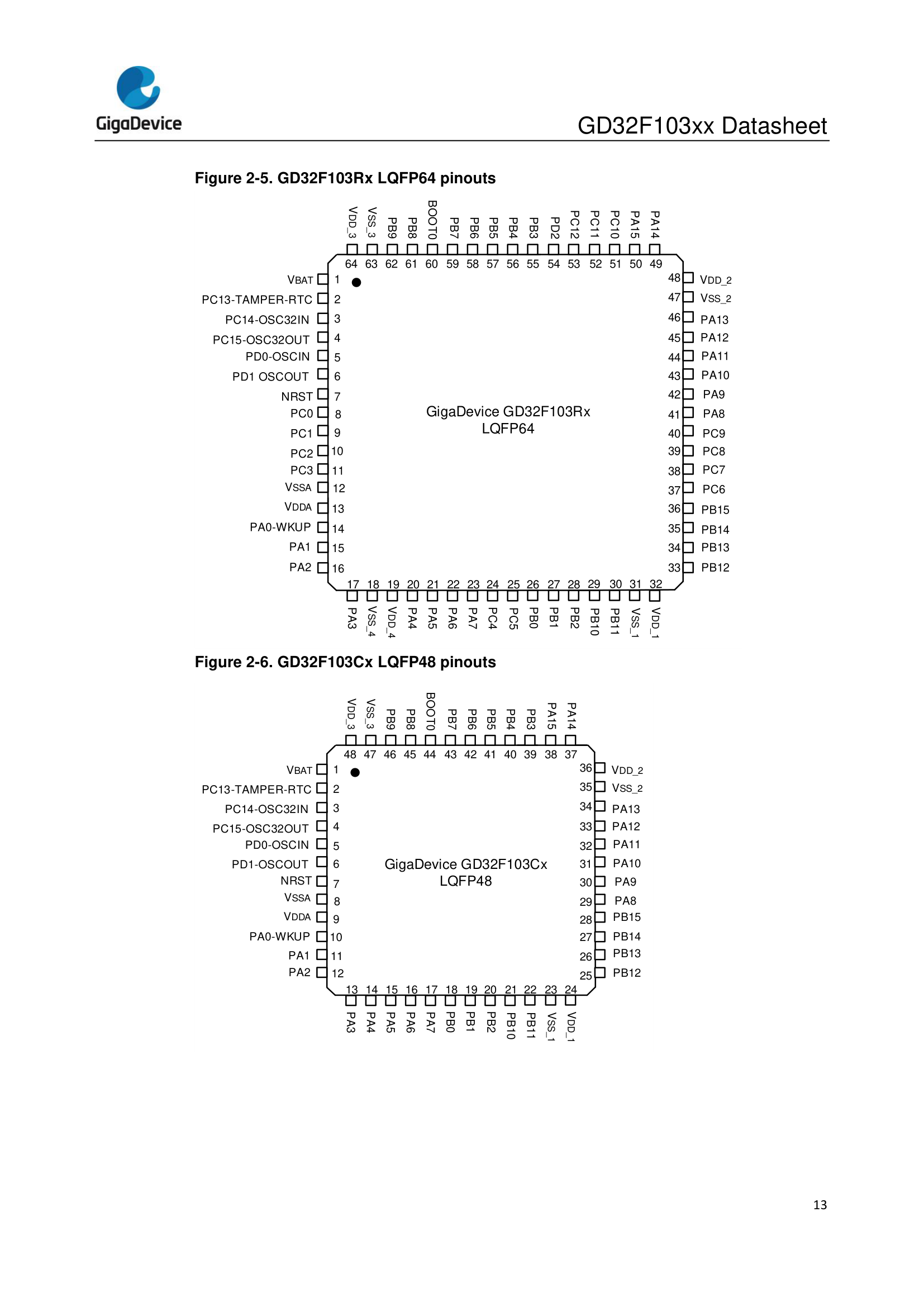
Pinout diagram
| Attr | Specs | verified |
|---|---|---|
mcu_cpu | Arm Cortex-M3, 32-bit, up to 108 MHz with zero-wait-state flash accesses (vs 72 MHz on the ST STM32F103 — see Features). Zero-wait applies to the first 256 KB of flash only (GD32F10x User Manual EN V2.3 §2.1, mirror). | ✔ |
gpu | none (MCU). | ? unverified |
ram | 6/10/20 KB SRAM on 16–128 KB parts (T/C/R/V 4/6/8/B); 48–96 KB on 256 KB–3 MB parts. Family max: 96 KB. | ? unverified |
storage | 16 KB to 3072 KB on-chip flash (family max 3 MB; Blue Pill parts 64/128 KB). Erase granularity is page-based: 1 KB pages on medium-density (MD) parts, 2 KB/4 KB pages on HD/XD/CL dual-bank parts ([GD32F10x User Manual §2.3.1]; the official SPL example uses #define FMC_PAGE_SIZE 0x400 = 1024 B (SPL V2.2.2 FMC example, mirror). Endurance 100 k cycles, data retention 20 y @125 °C, page erase 60–450 ms. | ✔ |
connectivity_radios | none integrated (no WiFi/BT/Ethernet on GD32F103; Ethernet MAC exists only on the GD32F107 sibling gd32mcu.com Cortex-M3 page). Wired: 1× USB 2.0 FS device (48 MHz clock derived from main PLL, HSE crystal required — datasheet §3.17), 1× CAN 2.0B, up to 3× SPI, 2× I2C, 3× USART + 2× UART, 2× I2S (8–192 kHz), SDIO. | ✔ |
gpio_analog | 26 GPIO (LQFP48) up to 112 (LQFP144), 5 V-tolerant I/O; up to 3× 12-bit SAR ADC @ 1 MSPS (ADC2 absent on C4/6/8/B), 16–21 channels, internal temperature sensor (ADC_IN16); 2× 12-bit DAC on C/D/E and larger parts; DMA0 7-ch + DMA1 5-ch; up to 10 general 16-bit timers + 2 advanced + 2 basic; RTC; EXMC external memory controller on LQFP100/144 parts. | ? unverified |
clocking | factory-trimmed internal IRC8M (±1 % @25 °C), HXTAL 4–16 MHz, PLL ×2–32, IRC40K + LXTAL 32.768 kHz for RTC/FWDGT. APB1 max 54 MHz, APB2 max 108 MHz, ADC clock ≤14 MHz. | ? unverified |
power | 2.6–3.6 V supply and I/O; VBAT 1.8–3.6 V. Run @108 MHz: typ 45.5 mA (all peripherals on) / 34 mA (off) on small parts; 66.3/41.2 mA on large parts; @72 MHz 30.7/45.0 mA. Standby ≈5.6–5.8 µA (RTC on); sleep wake-up 4.5 µs. | ? unverified |
temperature | −40 to +85 °C operating ("Industrial" grade ordering codes), storage −55 to +150 °C, TJ max 125 °C. | ? unverified |
boot | BOOT0 pins select main flash / system memory bootloader / SRAM; the system bootloader sits at 0x1FFF B000–0x1FFF F7FF and option bytes at 0x1FFF F800 (datasheet memory map) — note this differs from the STM32F103 system-memory layout. A 96-bit unique device ID and memory-density signature exist (User Manual §1.5.2 "Unique device ID (96 bits)"); > | ? unverified |
- Manufacturer: GigaDevice Semiconductor Inc. (Beijing, founded 2005; SSE:603986), a fabless Chinese vendor of NOR flash and GD32 MCUs (Wikipedia — GigaDevice, retrieved 2026-10-13).
- Year: the GD32 Cortex-M3 series was introduced in 2013, when GigaDevice entered the MCU market (Wikipedia — GigaDevice); GigaDevice's own GD32F103 migration app note AN001 v1.0 is dated Jan 14, 2013 (GD32F103xx AN001 Software Migration Guide). Western media coverage began in December 2015 (CNX Software).
- Status: active. The GD32F1/F2 (Cortex-M3) line is still listed on the official site among "more than 300 MCU models" (gd32mcu.com product page, retrieved 2026-10-13).
- Launch price: >
- Variants (ordering codes, official datasheet Rev 2.9): flash 16/32/64/128 KB parts GD32F103T4…TB (QFN36), C4…CB (LQFP48), R4…RB (LQFP64), V8/VB (LQFP100), plus 256 KB–3072 KB parts RC…RK, VC…VK, ZC…ZK (LQFP64/100/144) with 48–96 KB SRAM. The Blue-Pill-relevant parts are GD32F103C8T6 (64 KB, LQFP48) and GD32F103CBT6 (128 KB, LQFP48) — the 128 KB "CB" option matters because STM32F103 boards sold as "C8" often only expose 64 KB (all from GD32F103xx Datasheet Rev 2.9, mirrored here, retrieved 2026-10-13).
+ Strengths
- 108 MHz vs 72 MHz, zero-wait flash: the headline difference vs STM32F103 — 1.5× the clock with flash accesses at CPU speed (datasheet; CNX 2019: "compatible with STMicro STM32F103, but with a higher 108 MHz clock, and zero wait state internal flash… drop-in replacement… pin-to-pin compatible", retrieved 2026-10-13). Even at equal 72 MHz, Dhrystone measured 64.41 vs 48.81 VAX MIPS (GD32 vs STM32) thanks to zero-wait flash — Roger Clark, cited by CNX 2015.
- Pin-to-pin + firmware compatible with STM32F103: Olimex socketed a GD32F103RBT6 on its own STM32F103 board and it "passed all functional tests without any modifications", same tools and code (CNX 2015, Olimex test log).
- Flash far beyond STM32F103: up to 3 MB flash / 96 KB SRAM (STM32F103 tops out at 512 KB/64 KB), 2 KB/4 KB page erase + dual-bank on big parts, 1 KB pages on MD parts (User Manual §2.3.1) — finer-grained wear management than STM32F103's 16 KB sectors.
- 128 KB in the Blue Pill footprint: GD32F103CBT6 gives 128 KB flash in the LQFP48 package many "C8" Blue Pills ship with only 64 KB usable.
- Price: chips historically $0.70–$2.80 (2015, Taobao) — a major reason Grey-market Blue Pills switched to it ([CNX 2015]).
- RISC-V sibling: the GD32VF103 (same pinout class, RISC-V "Bumblebee" core @108 MHz) enabled boards like Sipeed Longan Nano — relevant if you want the footprint without the Arm license (CNX 2019).
− Weaknesses
- STM32 code needs two documented tweaks: GigaDevice's own AN001 migration note says HSE_STARTUP_TIMEOUT must be raised from 0x0500 to 0xFFFF (GD32 HSE start-up time differs) and the flash programming algorithm must be replaced in Keil/IAR projects (GD32F103xx AN001 §2–3, mirror). Symptom if ignored: hangs/failures waiting on HSE, or failed flashing with STM32 algorithms.
- Flash erase model differs: page erase (1 KB MD / 2 KB HD-XD) vs STM32F103's 16 KB sector erase (User Manual §2.3.1). STM32 code that erases "a sector" to rewrite one record will erase far less (or more) than expected on GD32 — data-logging corruption and failed porting are classic traps.
- Zero-wait only for the first 256 KB: "A long delay when CPU fetches the instructions out of the range" (User Manual §2.1) — the "108 MHz zero-wait" claim degrades on the 512 KB–3 MB parts beyond 256 KB.
- USB clock quirk: the USBD 48 MHz clock "is generated from the internal main PLL (the clock source must use a HSE crystal oscillator)" (datasheet §3.17) — USB won't come up from HSI-only clocking the way some STM32 designs tolerate.
- System bootloader relocated: GD32's bootloader region is 0x1FFF B000–0x1FFF F7FF (datasheet memory map), not STM32F103's 0x1FFF0000 — jump-to-bootloader code and linker assumptions break silently.
- Unique-ID caveats: the 96-bit unique ID exists (User Manual §1.5.2) but the datasheet marks the STM32-style signature window "Reserved"; >
- Quality/supply anecdotes: one engineer reported "out of 6 [GD32F103RCT6] chips, I only managed to flash one. And that one will not boot" during an STM32→GD32 switch (CNX 2022, APM32 article — translated first-hand account). Anecdotal, single source.
- You may already own one without knowing: most cheap "STM32F103C8T6" Blue Pills sold after ~2017 contain GD32 or other clones (Wikipedia — STM32; Greaseweazle STM32 Fakes). Detection: read the DBG ID code (0xE0042000, DBG_ID_ID_CODE in SPL gd32f10x_dbg.h) — GD32 and STM32 return different values.
- Ecosystem gaps: official ST tools/cores (STM32CubeMX, stm32duino core) don't target GD32 (see Systems); libopencm3 lacks GD32F103 in master (PR #1639 pending); MicroPython upstream has no GD32F103 port (community fork: CommunityGD32Cores/micropython).
- No default 108 MHz: out of reset the chip runs from IRC8M like STM32 from HSI; reaching 108 MHz requires correct PLL/HXTAL configuration — and some Blue Pill clones' crystals/boards are marginal at the higher clock. >
- Retour d'expérience expert expert — expert-microcontroleur
- Bonjour à tous. Après plusieurs mois d'utilisation intensive de la GD32F103, je confirme que l'attrait principal reste le rapport performance/prix. Les 108 MHz avec accès flash à vitesse CPU sont réels par rapport aux 72 MHz du STM32F103, ce qui donne un gain mesurable en Dhrystone. Cependant, atte… — expert-microcontroleur
- Salut, merci pour ce retour détaillé. Je suis justement en train de tester une Blue Pill 'clone' qui utilise apparemment cette puce. J'ai compilé un projet STM32 existant sans rien changer, sauf que j'ai remplacé le .hex. Au début ça semblait marcher, mais j'ai des coupures aléatoires en communicat… — maker-debutant-99
- Exactement pour le HSE, si le timeout n'est pas augmenté à 0xFFFF comme indiqué dans la note AN001, le MCu peut échouer à initialiser l'horloge externe si elle est un peu lente, d'où les instabilités. Pour le flash, oui, ne suppose pas que l'effacement d'une zone efface 16 Ko. Sur la GD32F103, c'es… — codeur-embed
Community feedback and projects
- Custom hardware GD32F103 (STM clone) broken after uploading Arduino sketch electronics.stackexchange.com
- GPIO Alternate Function GD32 electronics.stackexchange.com
- STM32 Clones: The Good, The Bad And The Ugly hackaday.com
- STM32F103 (Blue Pill): Dual/Synchronous ADC Mode Fails on Real Hardware community.st.com
Content not available yet.
- GD32F103xx_Datasheet_Rev2.9.pdf
- gd32mcu.com download center
- GD32F10x_User_Manual_EN_V2.3-3.pdf
- GD32F103xx-AN001-Software-Migration-Guide.pdf
- gigadevice-firmware-and-docs/GD32F10x
- Cortex-M3 series
- Vendor
- CommunityGD32Cores/ArduinoCore-GD32
- platform-gd32
- README
- PR #1639
- issue #1638
- libopencm3 GD32 status
- CNX 2015
- CNX 2019
- CNX 2022
- Wikipedia — GigaDevice/GD32
- Wikipedia — STM32
- Greaseweazle STM32 Fakes
- STM32 code needs two documented tweaks: GigaDevice's own AN001 migration note says HSE_STARTUP_TIMEOUT must be raised from 0x0500 to 0xFFFF (GD32 HSE start-up time differs) and the flash programming algorithm must be replaced in Keil/IAR projects (GD32F103xx AN001 §2–3, mirror). Symptom if ignored: hangs/failures waiting on HSE, or failed flashing with STM32 algorithms.
- Flash erase model differs: page erase (1 KB MD / 2 KB HD-XD) vs STM32F103's 16 KB sector erase (User Manual §2.3.1). STM32 code that erases "a sector" to rewrite one record will erase far less (or more) than expected on GD32 — data-logging corruption and failed porting are classic traps.
- Zero-wait only for the first 256 KB: "A long delay when CPU fetches the instructions out of the range" (User Manual §2.1) — the "108 MHz zero-wait" claim degrades on the 512 KB–3 MB parts beyond 256 KB.
- USB clock quirk: the USBD 48 MHz clock "is generated from the internal main PLL (the clock source must use a HSE crystal oscillator)" (datasheet §3.17) — USB won't come up from HSI-only clocking the way some STM32 designs tolerate.
- System bootloader relocated: GD32's bootloader region is 0x1FFF B000–0x1FFF F7FF (datasheet memory map), not STM32F103's 0x1FFF0000 — jump-to-bootloader code and linker assumptions break silently.
- Unique-ID caveats: the 96-bit unique ID exists (User Manual §1.5.2) but the datasheet marks the STM32-style signature window "Reserved"; >
- Quality/supply anecdotes: one engineer reported "out of 6 [GD32F103RCT6] chips, I only managed to flash one. And that one will not boot" during an STM32→GD32 switch (CNX 2022, APM32 article — translated first-hand account). Anecdotal, single source.
- You may already own one without knowing: most cheap "STM32F103C8T6" Blue Pills sold after ~2017 contain GD32 or other clones (Wikipedia — STM32; Greaseweazle STM32 Fakes). Detection: read the DBG ID code (0xE0042000, DBG_ID_ID_CODE in SPL gd32f10x_dbg.h) — GD32 and STM32 return different values.
- Ecosystem gaps: official ST tools/cores (STM32CubeMX, stm32duino core) don't target GD32 (see Systems); libopencm3 lacks GD32F103 in master (PR #1639 pending); MicroPython upstream has no GD32F103 port (community fork: CommunityGD32Cores/micropython).
- No default 108 MHz: out of reset the chip runs from IRC8M like STM32 from HSI; reaching 108 MHz requires correct PLL/HXTAL configuration — and some Blue Pill clones' crystals/boards are marginal at the higher clock. >
- Faire clignoter la LED PC13 debutant Schéma : IMG-gd32f103-debutant-1-clignotement-led.svg — carte GD32F103C8 compatible Blue Pill, LED embarquée PC13 clignotant à 1 Hz
- Bouton poussoir avec anti-rebond debutant Schéma : IMG-gd32f103-debutant-2-bouton-antirebond.svg — bouton poussoir sur PA0 avec résistance de pull-down, commande de la LED PC13 par toggling anti-rebondi
- Console série sur USART0 (PA9/PA10) debutant Schéma : IMG-gd32f103-debutant-3-console-serie-usart0.svg — convertisseur USB-série 3,3 V relié croisé à USART0 : PA9 en TX vers RX de l'adaptateur et PA10 en RX vers TX, masse commune
- Graduer une LED avec le PWM d'un timer intermediaire Schéma : IMG-gd32f103-intermediaire-1-pwm-led.svg — LED externe avec résistance 330 ohms sur PA6 pilotée en PWM par un timer du GD32F103C8, signal dent de scie annoté
- Lire un potentiomètre avec l'ADC 12 bits intermediaire Schéma : IMG-gd32f103-intermediaire-2-adc-potentiometre.svg — potentiomètre entre 3,3 V et masse, curseur relié à PA1, conversion ADC 12 bits du GD32F103C8 affichée sur la console série
- Afficheur OLED I2C SSD1306 intermediaire Schéma : IMG-gd32f103-intermediaire-3-i2c-oled-ssd1306.svg — module OLED SSD1306 0,91 pouce en I2C sur le bus du GD32F103C8 : SCL, SDA avec résistances de pull-up, VCC 3,3 V, adresse 0x3C
- Interruption EXTI + anti-rebond par timer avance Schéma : IMG-gd32f103-avance-1-exti-timer-debounce.svg — chronogramme EXTI sur PA0, timer 1 kHz, machine à états anti-rebond sans temporisation bloquante, LED PC13 commandée en SPL
- Acquisition ADC en DMA circulaire avance Schéma : IMG-gd32f103-avance-2-dma-adc.svg — flux ADC0 vers DMA0 canal 0 vers un tampon en SRAM en mode circulaire, sans intervention CPU, sur GD32F103C8
- Sommeil profond Stop et réveil par RTC avance Schéma : IMG-gd32f103-avance-3-stop-rtc-reveil.svg — GD32F103C8 en mode Stop, horloges coupées, RTC sur IRC40K réveillant le CPU toutes les 2 secondes, LED PC13 pulsée à chaque réveil
Code library — examples written for this board
clignotante.inoArduinobouton-led.inoArduinorespiration.inoArduinopotentiometre.inoArduinopont-uart.inoArduinooled-i2c.inoArduinodht22.inoArduinoservo.inoArduinomesure-frequence.inoArduinosommeil.inoArduino
Examples and repos found online
- CommunityGD32Cores/ArduinoCore-GD32 github.com
- CommunityGD32Cores/gd32-pio-projects github.com
- bmourit/ArduinoCore-MFL github.com