Efinix Sapphire RV64 : Configurable 64-bit RISC-V SoC for FPGAs
⚡ The essentials in 60 seconds
- architecture — 64-bit RISC-V
- core_count — 1 to 4 cores
- max_frequency — 400 MHz
- pipeline — 7-stage
- l2_cache — 64 KB to 512 KB (optional)
- on_chip_ram — 4 KB to 512 KB
- On this board : 9 tutorials · 10 code
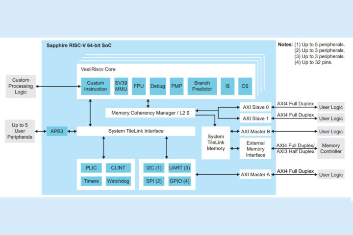
Imagine a world where the brain of a computer is not a fixed, immovable chip soldered onto a circuit board, but rather a flexible blueprint that you can reshape, scale, and tune to fit the exact needs of your project. This is the fundamental promise of the Efinix Sapphire RV64, a sophisticated system-on-chip design that transforms standard field-programmable gate arrays into powerful, customizable computing platforms. At its heart lies the VexiiRiscv core, a soft-core processor based on the open-source RISC-V architecture. Unlike traditional microcontrollers where the processor is hardwired into silicon, a soft-core is implemented using the programmable logic resources of an FPGA. This distinction is crucial for understanding the Sapphire RV64’s value proposition. It means that the processor itself is a piece of hardware description code that is synthesized onto the FPGA fabric. Consequently, engineers are not bound by the rigid specifications of a single chip. Instead, they can configure the processor’s capabilities, from the number of cores to the amount of memory, ensuring that they pay only for the performance and features they actually need, rather than carrying the overhead of unused hardware.
The Sapphire RV64 is built upon the 64-bit RISC-V instruction set architecture, a modern and open standard that has gained significant traction in the embedded and high-performance computing worlds. The core features a seven-stage pipeline, a design choice that balances complexity with frequency potential, allowing the processor to reach clock speeds of up to 400 MHz. This frequency is substantial for a soft-core implementation and provides a solid foundation for running complex applications. The architecture supports a rich set of instruction set extensions, specifically RV64IMACFD_Zba_Zbc_Zbs. For those less familiar with these acronyms, this translates to a processor that can handle integer arithmetic, multiply-divide operations, atomic instructions, compressed instructions for code density, and, crucially, both single and double-precision floating-point math. The inclusion of the Zba, Zbc, and Zbs extensions further enhances performance for specific bit-manipulation tasks, which are common in signal processing and cryptographic applications. This comprehensive instruction set ensures that the Sapphire RV64 is not just a simple controller, but a capable general-purpose computing engine.
One of the most compelling aspects of the Sapphire RV64 is its scalability, particularly regarding multi-core configurations. Depending on the size and resources of the underlying FPGA, engineers can instantiate between one and four cores. This flexibility allows for parallel processing, which is essential for modern applications that require multitasking or high-throughput data handling. Whether you are designing a control system that needs to manage multiple independent tasks simultaneously or a data processing unit that must crunch numbers in parallel, the ability to scale from a single core to a quad-core cluster provides a versatile solution. This scalability is supported by a robust memory subsystem that is equally configurable. On-chip RAM can be sized anywhere from 4 KB to 512 KB, offering a fast, low-latency storage area for critical code and data. For larger applications, the system supports external memory interfaces that can handle capacities ranging from 4 MB up to a massive 8 GB.
The external memory support is particularly noteworthy because it offers a choice of three different technologies: DDR3, LPDDR4x, and HyperRAM. Each of these technologies serves different needs. DDR3 is a well-established standard offering a balance of speed and cost, operating at 800 Mbps. LPDDR4x is a low-power variant that achieves much higher bandwidth, up to 3,200 Mbps, making it ideal for bandwidth-intensive applications where power efficiency is also a concern. HyperRAM, operating at 500 Mbps, offers a simpler interface with fewer pins, which can be advantageous in space-constrained designs. To further optimize performance, especially in multi-core scenarios, the Sapphire RV64 offers an optional shared L2 cache ranging from 64 KB to 512 KB. This cache sits between the fast L1 caches of the individual cores and the slower external memory, reducing latency and bandwidth pressure by storing frequently accessed data closer to the processors.
For operating system support, the architecture includes an optional SV39 Memory Management Unit. The MMU is a critical component for running modern operating systems like Linux, as it provides virtual memory capabilities, allowing the OS to manage memory efficiently and isolate processes from one another. Without an MMU, running a full-featured OS is difficult or impossible. By making the MMU optional, the Sapphire RV64 remains accessible for simpler real-time applications that do not require virtual memory, while still offering a path to full Linux support for more complex systems. This dual capability makes the platform suitable for a wide spectrum of applications, from bare-metal embedded control to sophisticated Linux-based edge computing devices.
Connectivity and peripheral support are handled through a comprehensive set of interfaces. The system provides up to 32 General Purpose Input/Output pins, which can be configured for various digital signal needs. For communication with other chips and modules, it includes five I2C masters, three SPI masters, and three UARTs. These interfaces are the workhorses of embedded systems, allowing the processor to communicate with sensors, displays, memory chips, and other peripherals. Additionally, the system supports AXI4 and APB3 bus interfaces, which are standard protocols for connecting to other IP cores within the FPGA. This standardization facilitates the integration of custom hardware accelerators or third-party IP blocks, enabling a true heterogeneous computing environment where software and hardware work together seamlessly.
Debugging is an often-overlooked but vital aspect of embedded development. The Sapphire RV64 supports standard RISC-V debugging protocols and provides up to four hardware breakpoints. Hardware breakpoints are essential for identifying issues in real-time systems where software breakpoints might alter timing or behavior. This level of debug support ensures that developers can effectively diagnose and resolve issues during the development phase, reducing time-to-market.
The Sapphire RV64 is designed to be compatible with Efinix’s Titanium, Topaz, and Trion FPGA families, specifically requiring devices of the T20 grade or higher. This compatibility ensures that there is a range of FPGA options available, from cost-effective mid-range devices to high-performance parts, allowing designers to match the FPGA size to their specific resource requirements. To implement this SoC, engineers must use the Efinity 2026.1 software suite or a more recent version. This requirement highlights that the Sapphire RV64 is a modern design leveraging the latest tools and features from Efinix, ensuring access to up-to-date synthesis, place-and-route, and verification capabilities.
In summary, the Efinix Sapphire RV64 represents a significant step forward in configurable computing. By combining the flexibility of a soft-core processor with the performance of modern RISC-V extensions, scalable memory subsystems, and robust peripheral support, it offers a powerful platform for developers who need more than what a fixed microcontroller can provide. It bridges the gap between simple microcontrollers and complex application processors, allowing for a tailored solution that optimizes cost, power, and performance. Whether you are building a smart sensor, a motor controller, or a Linux-based gateway, the Sapphire RV64 provides the architectural foundation to bring your vision to life with precision and efficiency. Its design philosophy emphasizes choice and adaptability, ensuring that the hardware can evolve alongside the software and application requirements throughout the product lifecycle.
| Attr | Specs | verified |
|---|---|---|
architecture | 64-bit RISC-V | ? unverified |
core_count | 1 to 4 cores | ? unverified |
max_frequency | 400 MHz | ? unverified |
pipeline | 7-stage | ? unverified |
l2_cache | 64 KB to 512 KB (optional) | ? unverified |
on_chip_ram | 4 KB to 512 KB | ? unverified |
external_memory_support | DDR3, LPDDR4x, HyperRAM | ? unverified |
max_external_memory | 8 GB | ? unverified |
gpio | Up to 32 | ? unverified |
interfaces | 5x I2C, 3x SPI, 3x UART | ? unverified |
isa_extensions | RV64IMACFD_Zba_Zbc_Zbs | ? unverified |
mmu | Optional SV39 | ? unverified |
compatibility | Efinix Titanium, Topaz, Trion FPGAs | ? unverified |
The Efinix Sapphire RV64 is a soft-core SoC based on the VexiiRiscv core, designed for Efinix Titanium, Topaz, and Trion FPGA families. It features a configurable 64-bit RISC-V architecture with up to 4 cores at 400 MHz, including vector extensions and an optional MMU for Linux support.
+ Strengths
["- Extensible 64-bit RISC-V architecture (RV64IMACFD_Zba_Zbc_Zbs) with optional SV39 MMU for Linux support.","- High memory flexibility with 4 KB to 512 KB on-chip RAM and external support up to 8 GB via DDR3, LPDDR4x, or HyperRAM.","- Modular configuration allowing 1 to 4 cores, with optional shared L2 cache and diverse peripheral interfaces (I2C, SPI, UART)."]
− Weaknesses
["- Requires Efinity 2026.1 or newer for design.","- Limited to Efinix FPGA series T20 and above.","- Performance heavily depends on the chosen configuration (core count, caches, enabled extensions)."]
- Retour d'expérience expert expert — expert-microdb
- J'ai intégré la Sapphire RV64 sur un Titanium T20. L'implémentation avec 2 cœurs à 350 MHz est fluide. La clé est la MMU SV39 : indispensable pour Linux. Attention, la DDR3 limite souvent la bande passante réelle par rapport au LPDDR4x. Efinity 2026.1 gère bien le pipeline 7 étages, mais le timing … — expert-microdb
- Bon retour. J'utilise cette carte pour un contrôleur industriel. Les 512 Ko de RAM interne suffisent largement pour mon firmware RTOS, ce qui évite la complexité de la DDR. Par contre, ne sous-estimez pas la config des masters I2C/SPI. Si vous activez les extensions FD, le placement routage explose… — membre-forum
Community feedback and projects
- Discussions Reddit — Sapphire RV64 reddit.com
- Articles CNX Software — Sapphire RV64 cnx-software.com
Content not available yet.
Content not available yet.
Content not available yet.
["- Not specified"]
- Getting Started with the Sapphire RV64 Board debutant Guide pas à pas pour alimenter, connecter et vérifier le fonctionnement de base de votre carte SoC RISC-V Efinix.
- Controlling GPIOs on Sapphire RV64 debutant Apprenez à configurer et piloter les broches d'entrée/sortie générales (GPIO) de votre SoC Sapphire RV64 pour interagir avec le monde physique.
- Simple UART Automation with Sapphire RV64 debutant Apprenez à configurer une interface UART pour envoyer des données sérialisées depuis le cœur RISC-V vers un terminal.
- Getting Started with Sapphire RV64 on Efinix FPGA intermediaire Guide étape par étape pour configurer, synthétiser et déboguer le premier bitstream du SoC RISC-V 64 bits sur une carte de développement Efinix.
- Configuring GPIOs and Driving Peripherals on Sapphire RV64 intermediaire Apprenez à configurer les broches GPIO du SoC Sapphire RV64 via Efinity pour interagir avec des composants externes comme des LED ou des capteurs.
- Deploying an IoT Node with Sapphire RV64: Network and Storage intermediaire Configurez un système embarqué complet sur FPGA Efinix en exploitant les interfaces AXI4 et les extensions RISC-V pour la gestion de données.
- Getting Started with Sapphire RV64 SoC on Efinix FPGA avance Guide avancé pour configurer et déployer le cœur VexiiRiscv Sapphire RV64 sur une carte Efinix.
- Mastering I/O on Sapphire RV64: GPIO and Protocols avance Configurez et pilotez les interfaces périphériques avancées (GPIO, I2C, SPI) du SoC Sapphire RV64 pour des interactions matérielles complexes.
- Deploying a real-time IoT gateway on Sapphire RV64 avance Configurez le SoC VexiiRiscv pour un traitement réseau critique avec DMA et gestion de la mémoire avancée.
Code library — examples written for this board
gpio_blink_riscv.inoC (RISC-V)uart_echo_riscv.inoC (RISC-V)spi_sensor_read.inoC (RISC-V)i2c_master_write.inoC (RISC-V)timer_interrupt_handler.inoC (RISC-V)i2c-bmp280-temperature-6.inoCspi-flash-storage-7.inoCpwm-buzzer-tone-8.inoCuart-console-log-9.inoCgpio-irq-interrupt-10.inoC